What is PCB panel? What factors should be considered?
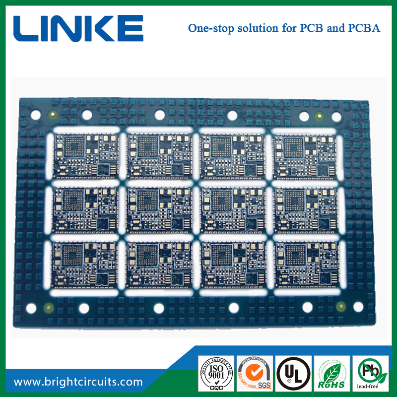
PCB panel is the process of combining multiple smaller, similarly shaped circuit boards together to form a larger PCB surface. The purpose of doing so is to reduce the loss of rohs 94v-0 pcb board, that is, to improve the utilization rate of PCB boards; Another reason is that it can increase the output efficiency of SMT patches.
Common types of PCB Panel boards
V-CUT panel: Cut a V-shaped groove between two PCBs, with a gap of generally 0.4mm, which is easy to break. When assembling boards, the edges of the two boards need to be merged together. Suitable for regular PCB boards, convenient for mechanical or automatic board splitting.
Matters needing attention:
The PCB thickness of the splicing board should be ≤ 3.5mm.
For PCBs that require automatic board splitting by machines, both sides of the V-CUT line are required to reserve a no less than 1mm prohibited area for component placement.
Considering the safety distance "S" from the edge of V-CUT to the edge of the line (or PAD), it is generally required that S ≥ 0.3mm.
Stamp hole panel board: A small piece of board is used to connect the edges of two boards, and there are many small holes at the connection, which are easy to break. The edge of the broken board looks like the edge of a stamp. Suitable for irregular PCB boards.
Matters needing attention:
The stamp holes should be non-metallic holes with a diameter of 1mm and a center distance of 1.6-2mm between the holes.
The stamp holes should be evenly distributed around each panel to avoid deformation caused by uneven stress on the PCB during soldering.
What does PCB Mirror-Board mean?
Mirror Board refers to the arrangement of the front and back sides of the same PCB board on the same panel, that is, the front and back designs of a PCB are mirrored and arranged on the same panel. This design method is commonly used for circuit boards with fewer components, such as mobile phone PCB boards, to fully utilize the capabilities of SMT production lines and improve production efficiency.
Mirror PCB board design can improve production efficiency as it allows for the simultaneous installation of components on both sides in a single production process, saving time and cost, and better utilizing board space to reduce waste. However, it also has some drawbacks, such as the complexity of the patch and the issue of uneven heat distribution. The position and orientation of certain components may increase the difficulty of SMT, and the thermal capacity of different components may lead to uneven heat during reflow soldering, requiring special thermal management measures.
What does PCB process edge refer to?
The process edge of PCB is to add a width of 5mm on each side or four sides of the board, mainly to leave a track transfer position for SMT surface mount machine, so that the PCB board can be accurately clamped and transferred by the machine.
Components that are too close to the track edge are prone to collision when the SMT surface mount machine suction nozzle picks up the components and attaches them to the PCB board, making it impossible to complete production. Therefore, a certain amount of process edge must be reserved. Similarly, it is also applicable to some plug-in components to prevent similar phenomena during wave soldering.
The process edge is not part of the PCB board and will be removed after production is completed. With panel assembly and process edge design, there is no need to open fixtures, which saves pre production preparation time and enables faster delivery.
Factors to Consider in Designing PCB Panels
Panel size:
Different surface mount factories have different requirements for the maximum and minimum dimensions of panel boards. Generally speaking, PCBs smaller than 50x50mm are recommended to be assembled to improve production efficiency. The maximum size that Linke Electronics can assemble is: double-sided board ≤ 1400 * 610mm, multi-layer board ≤ 1050 * 610mm.
Consider the borders and gaps of the PCB:
Reasonably set the gaps and borders between PCBs to facilitate cutting and assembly, while ensuring that they are not damaged during separation due to small gaps.
Component spacing and layout:
Ensure that the layout of components on each small PCB is reasonable, avoid interference between components, and ensure that components on each PCB do not affect each other.
Component arrangement and segmentation stress:
When designing a panel, the arrangement of components should avoid component cracking caused by splitting stress. The pre engraved line panel structure can minimize the warping deformation during board splitting and reduce the stress on components. Try not to place valuable components near the edge of the process to avoid damage during board splitting.
Panel size and form:
The size and form of the panel should be processed according to specific project requirements, and the appearance design should be as close to square as possible. It is recommended to use a 2 × 2 or 3 × 3 panel method, and it is not recommended to use Mirror-boards unless necessary. The square panel form can better utilize materials and production equipment, and improve production efficiency.
Benchmark design:
After the panel design, it is necessary to ensure that the reference point edge of the large board is at least 3.5mm away from the board edge (this is the minimum range for the machine to clamp the PCB board edge). The two diagonal reference points on the large board should not be symmetrically placed, and the reference points on the front and back should also not be symmetrically placed to use the device's own recognition function to prevent the PCB from entering the machine in reverse or reverse.
PCB thickness and panel strength:
When the thickness of the PCB is less than 1.0mm, the strength of the entire PCB will decrease with the addition of panel connection positions or V-cut slots. The depth of the V-cut groove is usually one-third of the thickness of the board, which can damage the middle support frame of the PCB and cause a decrease in strength. If fixtures are not used for support, it will have an impact on subsequent processes.
The position of the golden finger:
If there are gold fingers on the PCB, they are usually placed on the outer side of the board edge in the direction of the non clamp position. The gold finger edge cannot be connected or processed by panel boards to prevent damage to the gold finger during production and ensure its normal function.
Shijiazhuang Linke Electronics Tech Co.,Ltd
Tel: +86-13603214393
Email: [email protected]
Add: Room 1517,Building A,Lecheng Business Plaza,Huai'an west road,Qiaoxi district, Shijiazhuang City,Hebei Province,China.