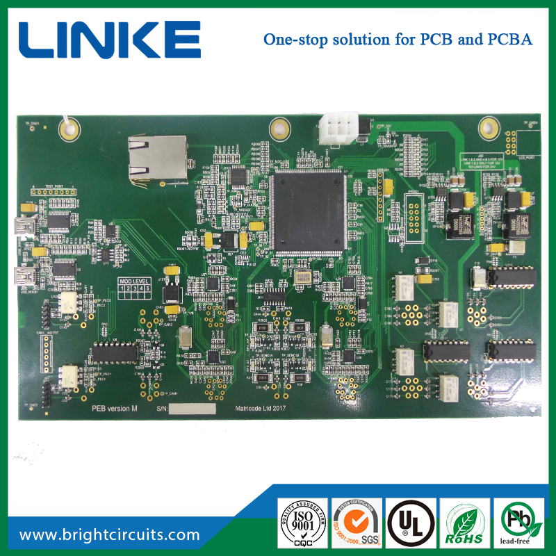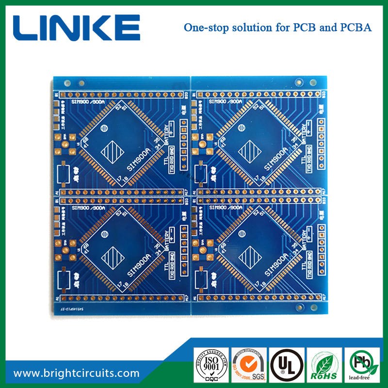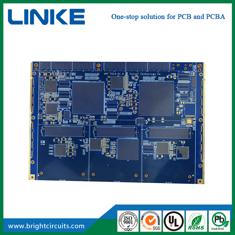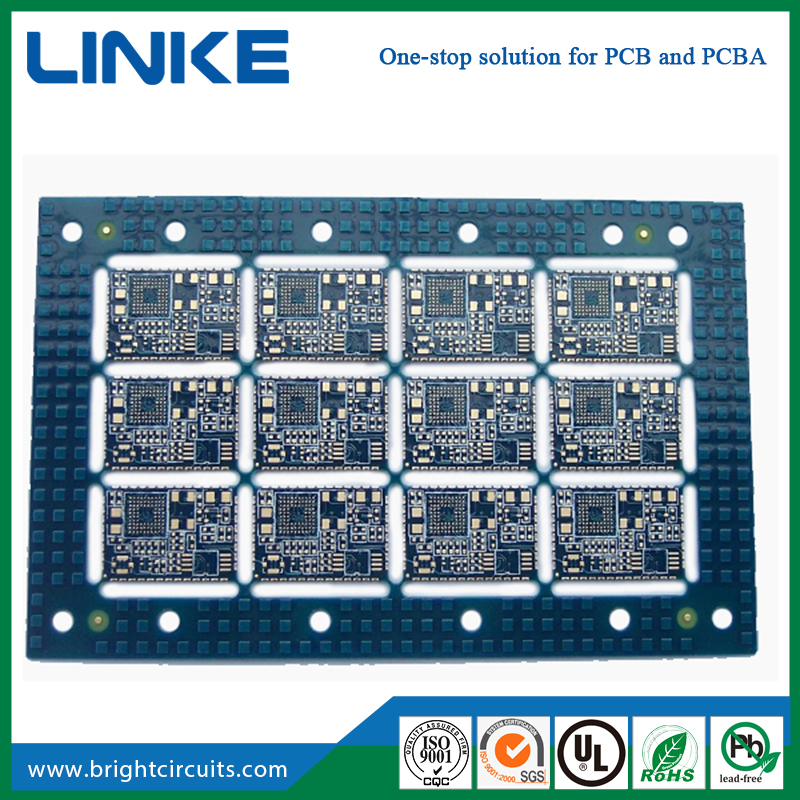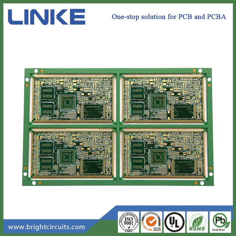
HDI is the English abbreviation of High Density Interconnector, that is, high-density interconnection board. It is a circuit board with a relatively high line distribution density using micro-blind and buried via technology.
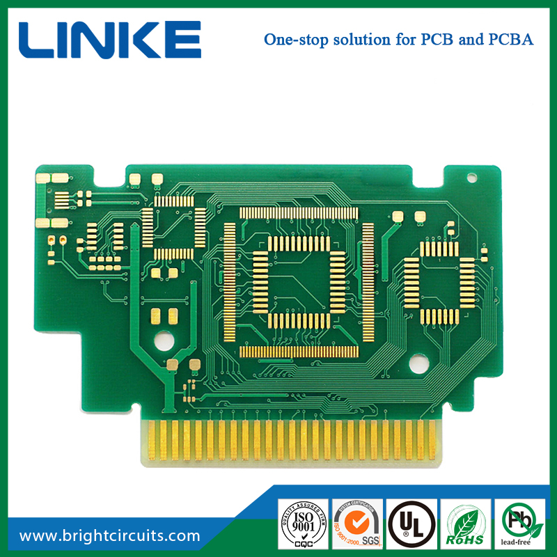
The HDI PCB board has inner and outer circuits. Drilling and metallization in the holes are used to connect the inner circuits of each layer.
Generally, build-up is used for manufacturing. The more build-up times, the higher the technical grade of the PCB panel. Ordinary HDI boards are basically layered once, and high-end HDI uses 2 or more layering techniques, while using advanced PCB technologies such as stacking holes, electroplating hole filling, and laser direct drilling.
Advantages of HDI circuit board:
It can reduce the cost of PCB: When the density of PCB increases to more than eight-layer board, it is manufactured with HDI, and its cost will be lower than that of the traditional and complex pressing process.
Increase circuit density: the interconnection of traditional circuit boards and parts
Conducive to the use of advanced construction technology
Have better electrical performance and signal accuracy
Better reliability
Can improve thermal properties
Can improve radio frequency interference/electromagnetic wave interference/electrostatic discharge (RFI/EMI/ESD)
Increase design efficiency
Shijiazhuang Linke Electronics Tech Co.,Ltd
Tel: +86-13603214393
Email: [email protected]
Add: Room 1517,Building A,Lecheng Business Plaza,Huai'an west road,Qiaoxi district, Shijiazhuang City,Hebei Province,China.