Methods and advantages of improving circuit wiring density for multi-layer PCB boards
In the field of electronic engineering, PCB is an indispensable part of electronic devices, and multi-layer PCB boards have received widespread attention due to their higher circuit wiring density and better performance. This article will explore in detail how multi-layer PCB boards can improve circuit wiring density and the advantages they bring.
The basic structure of multi-layer PCB boards:
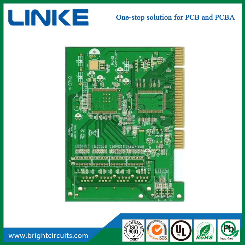
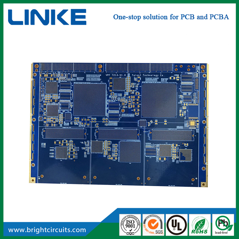
A multi-layer PCB board is composed of alternating layers of conductive materials (usually copper foil) and insulating materials (such as FR4) stacked together. By drilling holes and filling conductive materials between these layers, conductive paths connecting different layers can be formed, known as via. This design allows circuits to be laid out in three-dimensional space, greatly improving wiring density.
Methods for improving circuit wiring density:
1.Increase the number of layers: A significant advantage of multi-layer PCB boards is the ability to increase the number of layers as needed. By increasing the number of layers, more circuits can be arranged within a limited board area, thereby improving wiring density.
2.Optimize the design of vias: Vias are the key element connecting different layers of a multilayer PCB board. By optimizing the design of vias, such as reducing the diameter of vias, increasing the number of vias, and using vias filling techniques, the wiring density and circuit performance can be improved.
3. Fine wire width: The manufacturing accuracy of multi-layer PCB boards allows for the use of finer wires. By reducing the wire width, more circuits can be arranged in the same space, thereby increasing wiring density.
4. High density packaging technology: By using high-density packaging technologies such as BGA (Ball Grid Array) and CSP (Chip Scale Package), higher component density can be achieved on multi-layer PCB boards, further improving wiring density.
The advantages of multi-layer PCB boards in increasing circuit wiring density:
1. Reducing circuit board size: By increasing wiring density, the same circuit functions can be achieved on smaller circuit board sizes, which helps achieve miniaturization of electronic devices.
2. Improve signal transmission efficiency: The design of multi-layer PCB boards can reduce the length and complexity of signal transmission paths, thereby improving signal transmission efficiency.
3. Enhance circuit performance: Multilayer PCB boards can provide better electrical and thermal performance, which helps improve the overall performance of electronic devices.
4. Cost reduction: Although the manufacturing cost of multi-layer PCB boards is relatively high, their improved wiring density and circuit performance enable the overall design and manufacturing cost of electronic devices to be reduced.
Multi layer PCB boards effectively improve circuit wiring density by increasing the number of layers, optimizing Via design, using fine wire width, and adopting high-density packaging technology. This improvement not only helps to achieve miniaturization of electronic devices, but also improves signal transmission efficiency, enhances circuit performance, and reduces costs.
Linke Electronics,a professional Multilayer printed circuit board supplier from China.Welcome to place trial orders from us.
Shijiazhuang Linke Electronics Tech Co.,Ltd
Tel: +86-13603214393
Email: [email protected]
Add: Room 1517,Building A,Lecheng Business Plaza,Huai'an west road,Qiaoxi district, Shijiazhuang City,Hebei Province,China.