PCB defect detection methods and their advantages and disadvantages
With the continuous improvement of PCB accuracy, integration, complexity and quantity, PCB defect detection has become an important inspection content in the entire electronics industry.
Among them, traditional PCB defect detection technology, such as manual visual inspection, has been unable to meet the requirements of modern industrial production levels due to many shortcomings, so the development and application of new detection methods has become particularly important.
Manual visual subjective judgment method
With the help of a calibrated microscope or magnifying glass, the qualified rate of the circuit board is determined entirely based on the intuitive visual measurement of the operator, and the time for corrective operation is obtained.
Although this method has a low budget and does not require a test fixture, it has many disadvantages due to strong subjective judgment factors, low accuracy, high personnel costs, inconsistent defect detection, and difficulty in data collection.
Instrument online detection method
The online test method checks the open circuit, short circuit and faulty component functions of the circuit board soldering through simulation test and electrical performance test. When the component density on the circuit board is too large, it may be difficult to set the test points. At this time, boundary scan technology can be used, and all points can be detected by the online tester.
The online test technology based on electrical signals can detect the shape of the circuit board soldering very close to the actual situation. This method has the advantages of high conversion rate, low cost, wide defect detection coverage, and simple operation.
However, it requires a test fixture, which has the disadvantages of high fixture manufacturing cost, difficulty in use, and long programming and debugging time.
Functional test method
The system functional test method is to use special test equipment to test the functional modules of the circuit board in the middle and end of the production line, and to confirm the quality of the circuit board in a timely manner.
However, the functional test method cannot provide in-depth data such as component-level and pin-level diagnosis for process improvement, and requires specially designed test processes and special test equipment. The preparation of the test program is not only complicated, but also limited in promotion and use.
Visual inspection technology
Visual inspection technology covers the knowledge of electronics, mechanics, optics, computer software and hardware. It is an important branch of computer science and involves image processing, PC applications, pattern recognition, signal processing, artificial intelligence, mechatronics and other fields.
Based on the limitations of the above defect detection methods, the use of visual inspection technology to detect insufficient PCB soldering has become the main direction of current PCB defect detection research. The specific methods are as follows:
(1)Automatic optical inspection technology (AOI): It uses a variety of technologies such as automatic control, image analysis and processing, and computer application. Based on optical principles, it detects and processes soldering defects in production. It is a method for quickly and accurately detecting manufacturing defects. It mainly uses a camera to scan the PCB board, obtains the image of the solder joint area, and uses visual processing technology to quickly and accurately automatically detect soldering defects and extract corresponding features. Then, based on the extracted features and the standard features in the database, the type of soldering defects is determined and marked, and the quality problems are analyzed and the test result data is provided for relevant personnel to handle.
(2) Machine vision inspection technology (MVI): It uses the rapid development of CMOS and CCD cameras, image processing and pattern recognition technology, digital image sensors, and embedded technology (DSP, FPGA, ARM, etc.) to promote the advancement of machine vision inspection technology. In short, MVI is a new technology that uses machines to replace human eyes for various measurements and judgments. It integrates image processing technology (SRC), photoelectric detection technology (MSM) and computer application technology (Enterterms). MVI is introduced into industrial PCB inspection because it has significant advantages such as fast, non-contact, and good flexibility, and plays an important role in the inspection of the electronics manufacturing industry. At the same time, machine vision can also realize automatic defect detection of PCB bare boards, avoiding huge losses in the production process, and has a high practical economic value for the development of the electronics field.
(3) Computer vision inspection technology (AVI): Computer vision inspection technology based on computer vision research is an emerging industrial inspection technology. It uses image sensors to achieve three-dimensional measurement of the size and spatial position of the object being measured. By comparing the obtained data with standard and fault images, or directly extracting data from the image, the equipment is guided to act according to the inspection parameters. This intelligent inspection system based on visual sensors has the advantages of high time efficiency, simple structure, and strong anti-interference ability, which is very suitable for the requirements of modern industrial production.
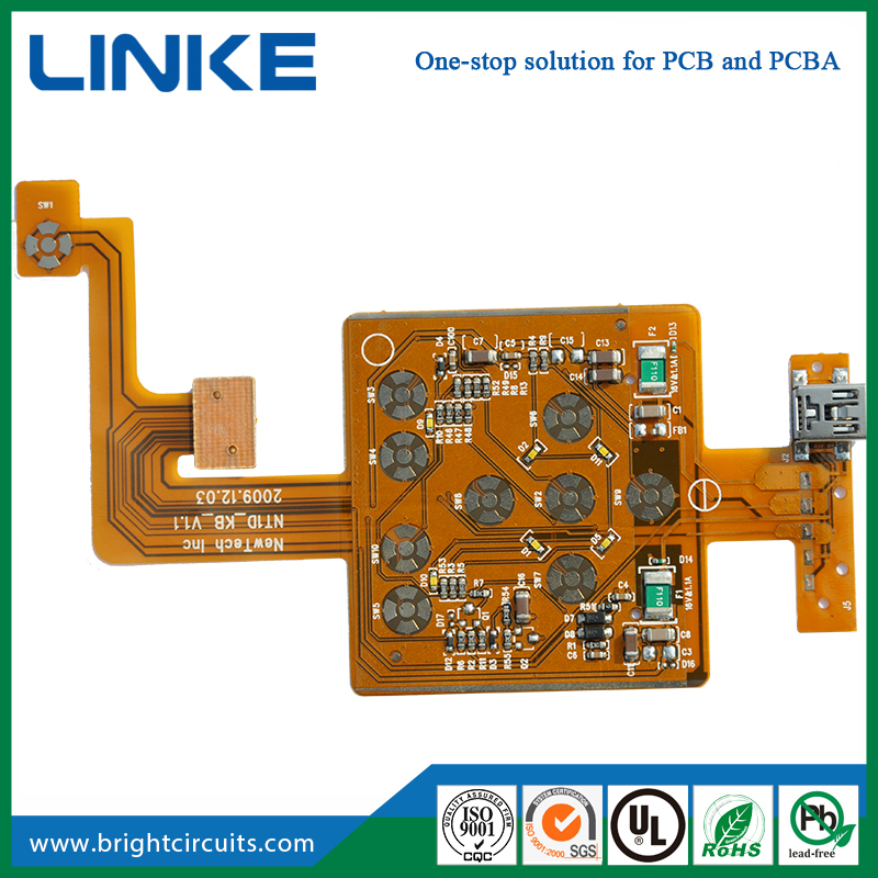
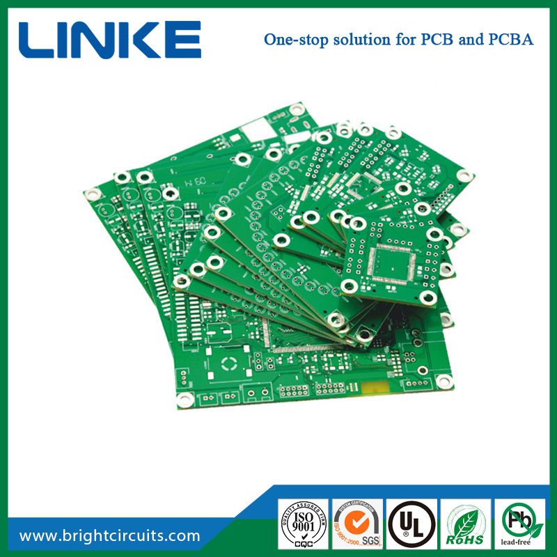
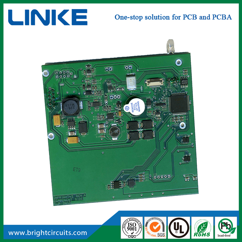
Shijiazhuang Linke Electronics Tech Co.,Ltd, we are one of the professional printed circuit board manufacturers in China.
Welcome to contact us for more information.
Shijiazhuang Linke Electronics Tech Co.,Ltd
Tel: +86-13603214393
Email: [email protected]
Add: Room 1517,Building A,Lecheng Business Plaza,Huai'an west road,Qiaoxi district, Shijiazhuang City,Hebei Province,China.