The demand for Prototype pcb assembly has always occupied an important position in the electronic assembly industry, such as the testing of new products, the quality testing of new cooperative SMT plants, etc.
The SMT factory itself attaches great importance to the product quality inspection of Prototype pcb assembly and large-scale PCB Assembly. The yield rate of the product is the best display of the PCB SMT factory.
Linke Electronics, a professional SMT PCBA factory, briefly introduces some common product inspection points.
Solder paste printing requirements:
1. The position of solder paste printing is moderate, which can be well pasted, and there is no phenomenon such as less tin and too much tin paste.
2. The solder paste points are well formed, and there can be no continuous tin, unevenness, etc.
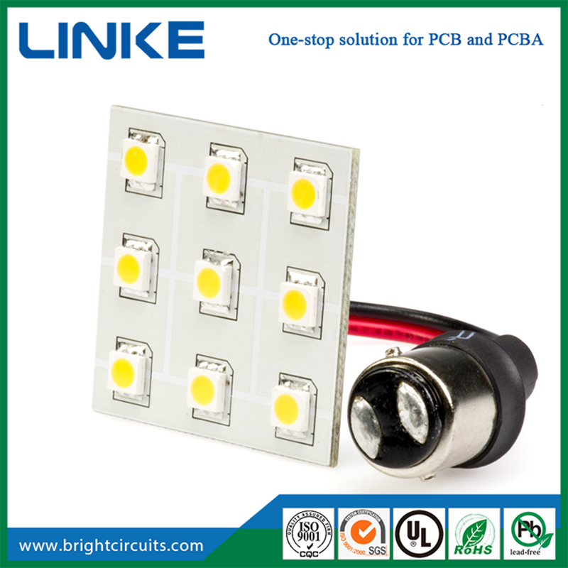
Component placement requirements:
1. The model and specification of the components at the mounting position should be correct; the components should be free of missing or wrongly pasted.
2. SMT components cannot be reversed.
3. SMD devices with polarity requirements should be installed according to the correct polarity marking.
4. Component placement should be neat and centered, without offset and skew.
Component soldering requirements:
1. There should be no solder paste and marks that affect the appearance on the circuit board for SMT PCB Assembly.
2. The bonding position of components should be free of rosin or flux that affects the appearance and soldering.
3. The tin points under the components are well formed, and there is no abnormal wire drawing or sharpening.
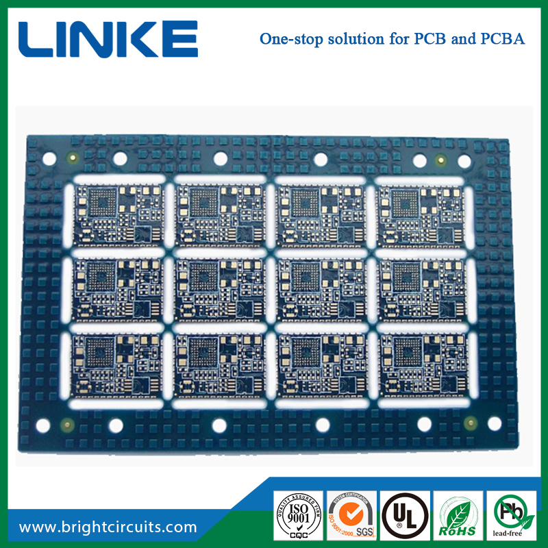
The appearance requirements of the circuit board:
1. There should be no cracks or cuts on the bottom of the PCB board, the surface of the PCB board, copper foil, lines, through holes, etc., and no short circuit caused by poor cutting.
2. The circuit board is parallel to the plane, and the board has no convex deformation.
3. The screen-printed text of the marked information characters has no blur, offset, reverse printing, offset printing, ghosting, etc.
4. There should be no swelling and foaming on the outer surface of the circuit board.
5. The aperture size requirements meet the design requirements.
Shijiazhuang Linke Electronics Tech Co.,Ltd, specializes in Prototype pcb assembly, providing electronic OEM processing, DIP plug-in processing, PCBA contracting, PCB circuit board manufacturing and other services, with advanced production equipment and perfect after-sales service system.
Shijiazhuang Linke Electronics Tech Co.,Ltd
Tel: +86-13603214393
Email: [email protected]
Add: Room 1517,Building A,Lecheng Business Plaza,Huai'an west road,Qiaoxi district, Shijiazhuang City,Hebei Province,China.