What is the difference between HDI circuit board and ordinary PCB?
Compared with ordinary circuit boards, HDI circuit boards have the following differences and advantages:
Size and Weight
HDI circuit board: Smaller and lighter. HDI PCB can achieve more compact design due to high-density wiring and finer line width and line spacing.
Ordinary PCB: Usually larger in size and heavier in weight, suitable for simpler and lower-density wiring needs.
Materials and Structure
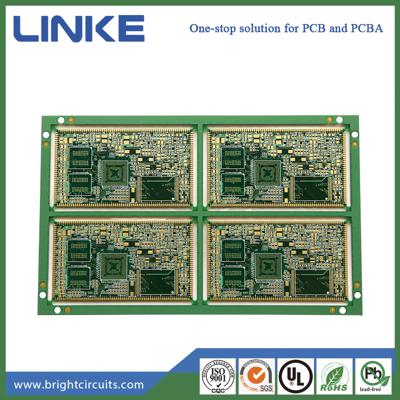
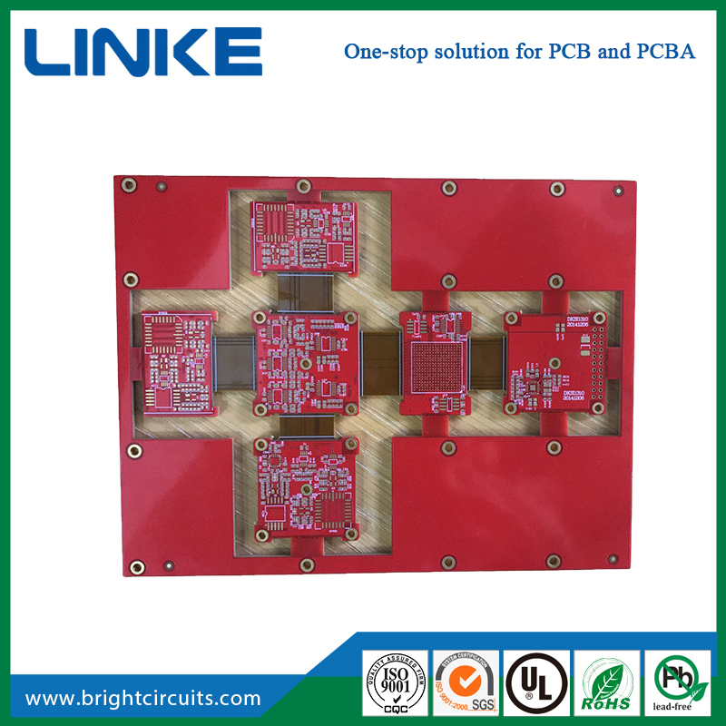
HDI circuit board: usually use double-sided board as core board, and then form a multi-layer structure through continuous lamination, which is called "BUM" accumulation of multiple layers (circuit packaging technology). The electrical connection between layers is achieved by using many tiny blind holes and buried holes.
Ordinary circuit board: The traditional multi-layer structure mainly uses through holes for inter-layer connection, and blind buried holes can also be used to achieve inter-layer electrical connection, but its design and manufacturing process are relatively simple, the aperture is larger, and the wiring density is lower, which is suitable for low to medium density application requirements.
Manufacturing process
HDI circuit board: Using laser direct drilling technology, it can achieve blind vias and buried vias with smaller apertures, with apertures less than 150um. At the same time, it has high requirements for hole position accuracy control, cost and production efficiency.
Ordinary circuit board: Mainly using mechanical drilling technology, the aperture and number of layers are usually larger.
Wiring density
HDI circuit board: The wiring density is higher, the line width and line spacing are usually no more than 76.2um, and the density of soldering contact points is greater than 50 per square centimeter.
Ordinary circuit board: The wiring density is lower, the line width and line spacing are wider, and the density of soldering contact points is lower.
Dielectric layer thickness
HDI circuit board: The dielectric layer thickness is thinner, usually less than 80um, and the requirements for thickness uniformity are higher, especially on high-density boards and package substrates with characteristic impedance control.
Ordinary circuit board: The dielectric layer thickness is thicker, and the requirements for thickness uniformity are relatively low.
Electrical properties
HDI circuit board: has better electrical performance, can enhance signal strength and reliability, and has significant improvements in radio frequency interference, electromagnetic wave interference, electrostatic discharge, thermal conductivity, etc.
Ordinary circuit boards: relatively low electrical performance, suitable for applications that do not require high signal transmission.
Design flexibility
Due to its high-density wiring design, HDI circuit boards can achieve more complex circuit designs in a limited space. This gives designers greater flexibility when designing products, and allows them to add functionality and performance without increasing size.
Although HDI circuit boards have obvious advantages in performance and design, the manufacturing process is relatively complex and requires high equipment and technology. Laser drilling, precision alignment, micro blind via filling and other processes require high-level technical support, which also leads to higher production costs for HDI circuit boards.
Compared with ordinary circuit boards, HDI circuit boards have higher wiring density, better electrical performance and smaller size, but their manufacturing process is complex and the cost is high. The overall wiring density and electrical performance of traditional multi-layer circuit boards are not as good as HDI circuit boards, and they are suitable for medium and low density application requirements.
Shijiazhuang Linke Electronics Tech Co.,Ltd
Tel: +86-13603214393
Email: [email protected]
Add: Room 1517,Building A,Lecheng Business Plaza,Huai'an west road,Qiaoxi district, Shijiazhuang City,Hebei Province,China.