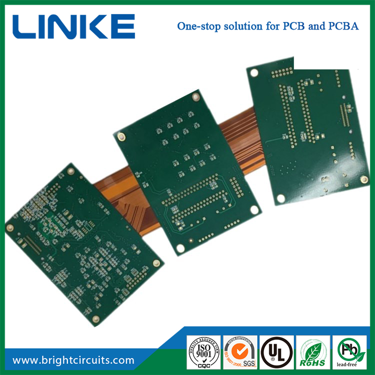
LATEST MATERIAL AND CONSTRUCTION METHODS PROVIDE THE HIGHEST QUALITY RIGID-FLEX PCB'S
With the demand for portable electronics ever increasing, the need to produce more compact devices with ever-increasing capabilities calls for engineering solutions that combine functionality with flexibility.
Rigid-Flex circuits can be shaped to fit where no other design solution can. They are an integrated hybrid of printed circuit board and flex circuit technology and exhibit the benefits of each. This allows substantially greater freedom of packaging geometry and a significant reduction of interconnects while retaining the precision, density and repeatability of printed circuit board technology.
Applications of Rigid-Flex circuits can be found throughout the electronics industry and in the most demanding applications including aerospace, medical and military.
Rigid-Flex circuit design has evolved significantly over the past decade. Modern designs require the rigid areas to be fully capable "rigid" boards. The same limits of complexity and density are pushed as in modern PCB's including: fine lines/spacing, high aspect ratio vias, blind and buried vias, high layer counts (20+), higher operating temperatures, and RoHS assembly compliance.
However, some of these advances created potential via and plated hole reliability issues. Older design methods used materials and constructions containing many layers of "adhesives" within the rigid area constructions. Due to adhesives having a high coefficient of thermal expansion (10 to 20 times that of FR-4), vias are placed under a significant amount of stress during thermal cycles that occur during RoHS assembly, multiple assembly cycles, and higher system and component operating temperatures. The use of adhesives within the rigid areas may cause cracks to form in the copper plating within via holes
Adhesives, within a rigid-flex design, may come from any of three sources: the copper clad flex laminate itself, the coverlay construction method used and the material used to bond the rigid and flex layers into the final structure. To solve the issue of via reliability, manufacturers, material suppliers and industry standards organizations have worked together to develop solutions and specifications that eliminate or minimize the use of adhesives in these areas.
To address the use of adhesives in copper clad flex laminate, "adhesiveless" constructions were developed. Previously, copper layers were bonded to the polyimide core with either an acrylic or modified epoxy adhesive (Figure 2a). An adhesiveless laminate has the copper directly attached to the polyimide core (Figure 2b). Eliminating the adhesive bond layers allows for thinner constructions and more flexible design with vastly improved reliability. In addition adhesiveless copper clad laminates have higher operating temperature ratings, higher copper peel strengths, and the desired reduced Z-Axis thermal expansion stress on vias.
Coverlay constructions also previously presented a problem in rigid-flex designs. Older methods use full coverage coverlays that extend throughout the entire rigid area(s). Vias and plated though holes would then be exposed to the excessive Z-Axis thermal expansion stress applied by the coverlay adhesive. To solve this issue, selective coverlay constructions were developed so that coverlays are restricted to the exposed flex areas only and have a maximum 0.050" interface within the rigid areas. (Figure 3). PTH and via holes are restricted from this interface area.
Lastly, rigid and flex layers are now laminated into the final structure, using high temp no-flow FR4 prepregs rather than layers of flex adhesives. This provides a structure as dimensionally stable in the Z-Axis as standard rigid PCB designs.
IPC 2223C Sectional Design Standard for Flexible Printed Boards lists all of the above as key elements in the design of a reliable rigid-flex design that meets today's requirements.
Linke Electronics manufactures single, double, and multi-layer flex circuits using modern rigid-flex materials and construction. Designs comply with IPC 2223C standards, which define the elimination/minimization of adhesive use within rigid areas, use of adhesiveless based substrates, and use of selective/partial coverlay construction.Linke Electronics's design review and quoting process, specifications, materials, and construction are carefully examined in order to minimize and eliminate any technical issues. Areas of opportunity for improved reliability, functionality, and cost reductions are also identified to generate an accurate quote that is based on a manufacturable, reliable and cost effective design.
