PRINTED CIRCUIT BOARD SURFACE FINISHES – ADVANTAGES AND DISADVANTAGES
Anyone involved within the printed circuit board (PCB) industry understand that PCB's have copper finishes on their surface. If they are left unprotected then the copper will oxidize and deteriorate, making the circuit board unusable. The surface finish forms a critical interface between the component and the PCB. The finish has two essential functions, to protect the exposed copper circuitry and to provide a solderable surface when assembling (soldering) the components to the printed circuit board.
Hot Air Solder Leveling (HASL) was once the tried and true method of deliver consistent assembly results. However, the ever-increasing circuit complexity and component density has stretched the capabilities of even horizontal solder levelling systems to their limits.
As component pitches became finer and a need for a thin coating became greater, HASL represented a process limitation for PCB manufacturers. As an alternative to HASL, alternative coatings have been around for several years now, both electrolytic and immersion processes.
Listed below are some more common surface finishes used in PCB manufacturing.
HASL / Lead Free HASL
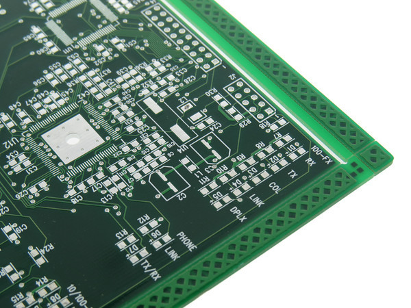
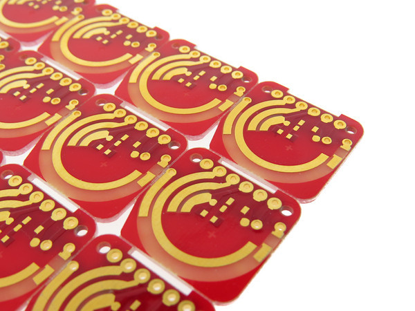
HASL is the predominant surface finish used in the industry. The process consists of immersing circuit boards in a molten pot of a tin/lead alloy and then removing the excess solder by using 'air knives', which blow hot air across the surface of the board.
One of the unintended benefits of the HASL process is that it will expose the PCB to temperatures up to 265°C which will identify any potential delamination issues well before any expensive components are attached to the board.
Printed Circuit Board with HASL / Lead Free HASL Surface Finish
Advantages:
· Low Cost
· Widely Available
· Re-workable
· Excellent Shelf Life
Disadvantages:
· Uneven Surfaces
· Not Good for Fine Pitch
· Contains Lead (HASL)
· Thermal Shock
· Solder Bridging
· Plugged or Reduced PTH's (Plated Through Holes)
Immersion Tin
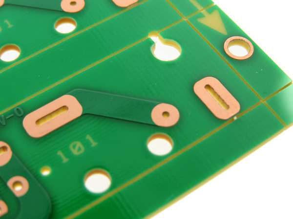
According to IPC, the Association Connecting Electronics Industry, Immersion Tin (ISn) is a metallic finish deposited by a chemical displacement reaction that is applied directly over the basis metal of the circuit board, that is, copper. The ISn protects the underlying copper from oxidation over its intended shelf life.
Copper and tin however have a strong affinity for one another. The diffusion of one metal into the other will occur inevitably, directly impacting the shelf life of the deposit and the performance of the finish. The negative effects of tin whiskers growth are well described in industry related literature and topics of several published papers.
Printed Circuit Board with Immersion Tin Surface Finish
Advantages:
· Flat Surface
· No Pb
· Re-workable
· Top Choice for Press Fit Pin Insertion
Disadvantages:
· Easy to Cause Handling Damage
· Process Uses a Carcinogen (Thiourea)
· Exposed Tin on Final Assembly can Corrode
· Tin Whiskers
· Not Good for Multiple Reflow/Assembly Processes
· Difficult to Measure Thickness
OSP / Entek
OSP (Organic Solderability Preservative) or anti-tarnish preserves the copper surface from oxidation by applying a very thin protective layer of material over the exposed copper usually using a conveyorized process.
It uses a water-based organic compound that selectively bonds to copper and provides an organometallic layer that protects the copper prior to soldering. It's also extremely green environmentally in comparison with the other common lead-free finishes, which suffer from either being more toxic or substantially higher energy consumption.
Printed Circuit Board with OSP / Entek Surface Finish
Advantages:
· Flat Surface
· No Pb
· Simple Process
· Re-workable
· Cost Effective
Disadvantages:
· No Way to Measure Thickness
· Not Good for PTH (Plated Through Holes)
· Short Shelf Life
· Can Cause ICT Issues
· Exposed Cu on Final Assembly
· Handling Sensitive
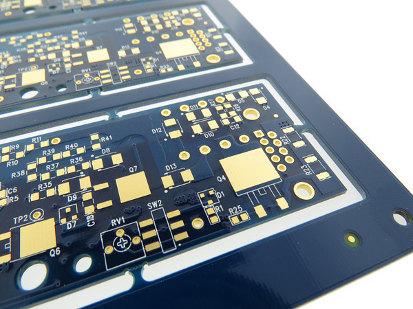
Electroless Nickel Immersion Gold (ENIG)
ENIG is a two layer metallic coating of 2-8 μin Au over 120-240 μin Ni. The Nickel is the barrier to the copper and is the surface to which the components are actually soldered to. The gold protects the nickel during storage and also provides the low contact resistance required for the thin gold deposits. ENIG is now arguably the most used finish in the PCB industry due the growth and implementation of the RoHs regulation.
Printed Circuit Board with Electroless Nickel Immersion Gold (ENIG) Surface Finish
Advantages:
· Flat Surface
· No Pb
· Good for PTH (Plated Through Holes)
· Long Shelf Life
Disadvantages:
· Expensive
· Not Re-workable
· Black Pad / Black Nickel
· Damage from ET
· Signal Loss (RF)
· Complicated Process
Gold – Hard Gold
Hard Electrolytic Gold consists of a layer of gold plated over a barrier coat of nickel. Hard gold is extremely durable, and is most commonly applied to high-wear areas such as edge connector fingers and keypads.
Unlike ENIG, its thickness can vary by controlling the duration of the plating cycle, although the typical minimum values for fingers are 30 μin gold over 100 μin nickel for Class 1 and Class 2, 50 μin gold over 100 μin nickel for Class 3.
Hard gold is not generally applied to solderable areas, because of its high cost and its relatively poor solderability. The maximum thickness that IPC considers to be solderable is 17.8 μin, so if this type of gold must be used on surfaces to be soldered, the recommended nominal thickness should be about 5-10 μin.
Printed Circuit Board with Gold – Hard Gold Surface Finish
Advantages:
· Hard, Durable Surface
· No Pb
· Long Shelf Life
Disadvantages:
· Very Expensive
· Extra Processing / Labor Intensive
· Use of Resist / Tape
· Plating / Bus Bars required
· Demarcation
· Difficulty with Other Surface Finishes
· Etching Undercut can Lead to Slivering / Flaking
· Not Solderable Above 17 μin
· Finish Does Not Fully Encapsulate Trace Sidewalls, Except in Finger Areas
Conclusion
It is important to select the appropriate surface finish for your project by considering the various options while factoring in performance requirements and material costs.
For an example, if you are looking for the lowest cost then Tin-Lead HASL might seem like a good choice, but it is not suitable for RoHS-compliant products. If your product does require RoHS, you might consider lead-free HASL. That is only if there are no fine pitch components, since LFHASL cannot be applied perfectly flat. If your design needs to be RoHS compliant and does use fine pitch components, then you'll need to select a flat, lead-free finish, such as Immersion Silver or ENIG. Bear in mind that doing so will necessitate the use of more costly high temperature laminate.
Unsure of what you will need? Consult with a PCB fabricator prior to you making a selection. This will ensure that the combination of the surface finish and material will result in a high-yielding, cost-effective design that will perform as expected.