The Internal Architecture of multilayer circuit board: Entering the World of Circuit Board Design
The design of multilayer circuit board is an indispensable and important part of modern electronic products.
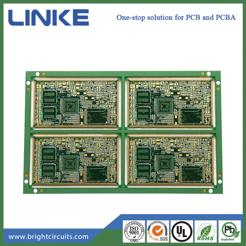
In the production process of multilayer circuit board, the processing of circuits is not much different from that of single-layer or double-layer PCB. The biggest difference lies in the process of vias.
Circuits are usually formed by etching, while vias need to be drilled first and then copper plated to form a passage. There is no necessary connection between through-hole boards and the number of layers. The number of layers of through-hole boards can be few or many.
Type of via:
Through-hole board is the most common type of via.
From the first layer to the last layer. Whether it is the external circuit or the internal circuit, the hole is connect, and this board is called a through-hole board.
In HDI board, the laser hole process is used. Laser holes can only penetrate glass fiber boards, not metal copper. Therefore, the laser holes on the outer surface will not affect other internal circuits, which makes the design of HDI board more compact.
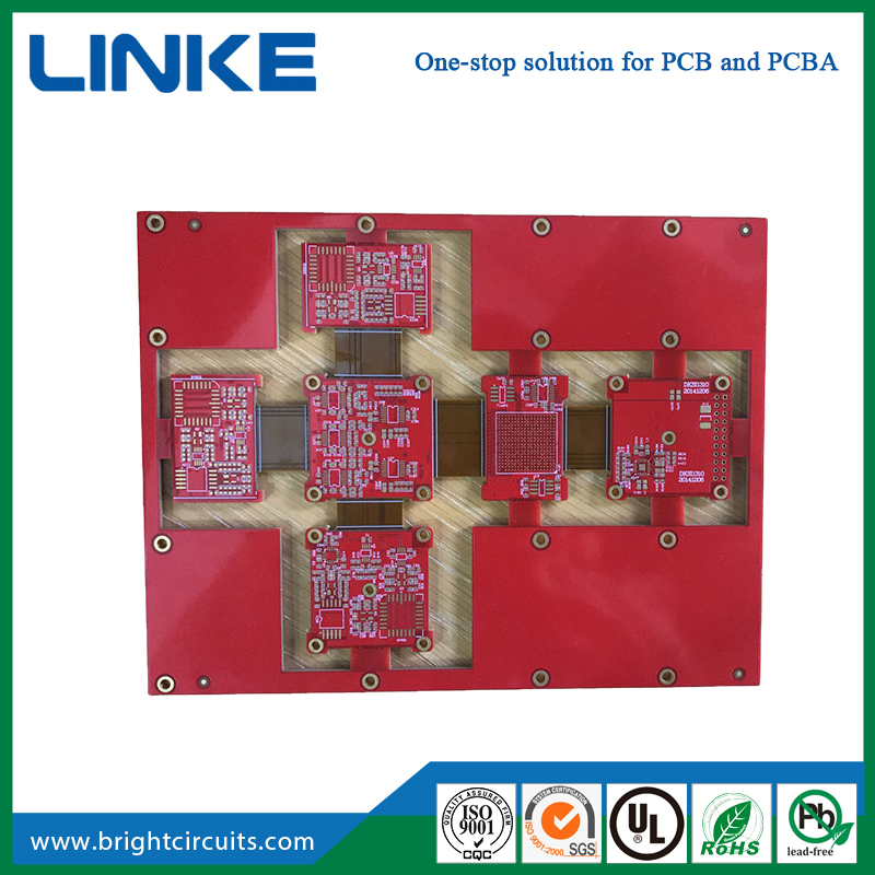
With the development of technology, more complex designs have emerged, such as stacked perforated boards and arbitrary layer interconnected boards.
The two layers of laser holes in the stacked perforated board will overlap, and the circuit will be more compact. However, the manufacturing process is also more complicated and the price is higher.
The arbitrary layer interconnected board has laser holes on each layer, which makes the routing and drilling very free and flexible, but due to the difficulty of manufacturing, the price is very expensive.
Application of multilayer circuit board:
In practical applications, different types of PCBs are suitable for different product levels.
For example, 8-bit MCU products usually use 2-layer through-hole boards, while 32-bit MCU-level smart hardware uses 4-6-layer through-hole boards. Linux and Android-level smart hardware usually use 6-layer through-hole to 8-layer first-order HDI boards, while compact smartphone products use 8-layer first-order to 10-layer second-order circuit boards.
Although the design of multi-layer PCBs may be a headache, it is an indispensable foundation for modern electronic products.
From through-hole boards to HDI boards to more complex stacked holes and arbitrary-layer interconnection boards, each design is constantly driving the development of electronic technology.
Whether it is for a more compact design or for more flexible routing, multi-layer PCBs are one of the keys to the success of modern electronic products.
If you want to build advanced electronic products, Shijiazhuang Linke Electronics Tech Co.,Ltd is your best choice! As an industry-leading multi-layer PCB manufacturer, we have rich experience and a professional team to tailor a variety of complex PCB solutions for you. Our HDI board technology makes your circuit boards more compact and more powerful. Whether you are developing smart hardware, high-performance servers, or innovative mobile devices, we can meet your needs.
In the future technological world, multi-layer PCBs will surely play a more important role and bring us more surprises and possibilities.
Shijiazhuang Linke Electronics Tech Co.,Ltd
Tel: +86-13603214393
Email: [email protected]
Add: Room 1517,Building A,Lecheng Business Plaza,Huai'an west road,Qiaoxi district, Shijiazhuang City,Hebei Province,China.