PCB Gold Finger Interpretation: Important Details You Need to Know
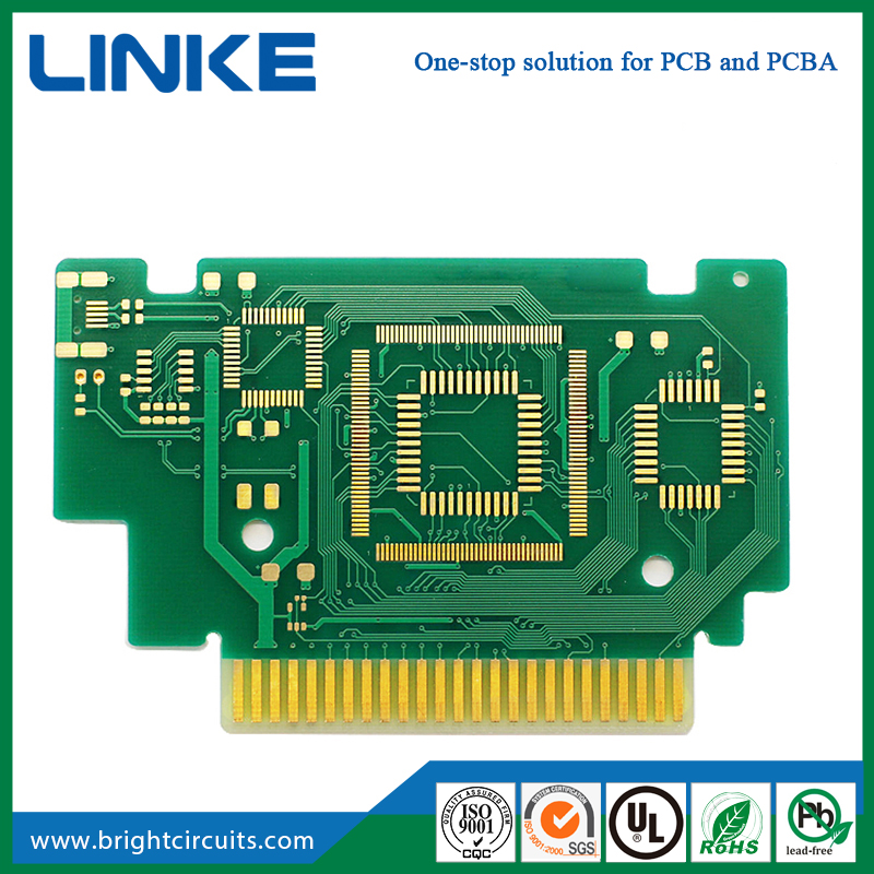
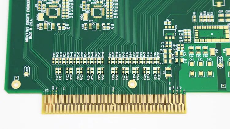
Gold fingers are narrow, long and thin connection points located on the edge of a circuit board. They are used to connect different circuit boards or devices to achieve data, electrical signals and power transmission. They provide a physical interface that allows connectors on other boards to contact them. Gold fingers can be used in devices such as smartphones and smart watches, and can also be used as adapters to transmit network data.
PCB Gold Finger Design Notes
Never design pads or screen printing near gold fingers, which will cause uneven gold finger connection area, which may affect the insertion and connection of gold fingers, and even cause poor connection or damage.
Gold fingers should be at the edge of the circuit board so that the gold fingers can be properly aligned and connected with the connectors of other devices or circuit boards.
PTH holes should be avoided from being placed near gold fingers, otherwise it may cause uneven gold finger connection area or produce additional metal residue, which will affect the insertion and connection of gold fingers.
When designing PCB gold fingers, it is recommended to use gold plating, which is more wear-resistant when the connector contacts. Although immersion gold can also be used and is more cost-effective than gold plating, it has poor resistance to wear.
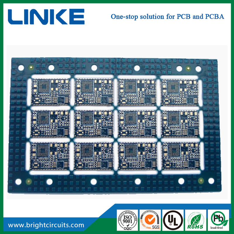
In order to ensure that the gold fingers and slots can fit correctly, each PCB must be inspected. This process usually requires inspection with a magnifying glass, and defect testing is also required so that subsequent functional tests can proceed normally.
What is PCB gold finger chamfering?
Chamfering is to ensure that the connector can be inserted quickly. The edge of the connector is chamfered at an angle of 30 to 45 degrees to prevent the gold finger from scratching the card slot or exposing the copper during the plug-in process. Chamfering is usually performed after the pad cover is coated and before surface treatment.
Chamfering is necessary for circuit boards with longer gold fingers. Doing so helps to connect them together to form a whole, and is also useful when a specific size of the edge connector is required. During the chamfering process, the gold fingers must be able to fit together easily, otherwise it may cause the edge connector to not fit completely.
Precautions for PCB gold fingers
When designing PCB gold fingers, there are some design specifications that require special attention. First, copper should be avoided at the edge of the PCB to prevent copper exposure during chamfering.
In addition, a distance of 1 mm should be maintained between the gold finger and the PTH hole, while the minimum distance between the gold finger and the edge of the circuit board should be 0.5 mm. Failure to comply with these spacing requirements may cause the circuit board to be prone to failure.
Standards that PCB gold fingers should follow
Chemical composition
Gold plating should contain 5 to 10% cobalt. This helps achieve maximum hardness on the edge of the PCB gold finger.
Thickness of gold fingers
Gold fingers are usually between 2 and 50 micro-inches thick, but they are often manufactured in standard thicknesses, such as 0.031 inches, 0.062 inches, 0.093 inches, and 0.125 inches.
Visual test
To ensure that the contact edge of the gold finger is smooth and clean, and there is no excess plating, a magnifying glass can be used for inspection.
Tape test
This is to ensure that the gold plating can make good contact with other contacts. The test is to stick a piece of tape on the contact edge, then remove it and check whether there is any plating residue on the tape. If there is metal residue on the tape, it means that the gold plating does not meet the requirements, and the subsequent insertion and removal steps may be affected.
On some circuit boards, the length of the gold fingers is different, such as the gold fingers on the memory card is a good example. In this case, the device connected by the long gold finger must be powered first, and then connected to the device on the short gold finger connector. When designing these gold fingers, avoid confusion to avoid short circuits.
For waterproof and durable electronic products, it is recommended to use segmented gold fingers, which have different lengths and some gold fingers may be disconnected inside.
Application of PCB Gold Fingers
The main purpose of gold fingers is to act as a connector between two circuit boards to transmit signals. They can also be used to make special adapters to facilitate the connection of various function-enhancing devices to computers.
In addition, gold fingers can also be used as connection points, such as connecting slots on the motherboard to attached circuit boards. The function of gold fingers is to transmit signals between computers, external devices or internal cards.
In addition, gold fingers can also be used as external connection points to connect circuit boards and other mechanical devices, which is common in computerized industrial applications.
Shijiazhuang Linke Electronics Tech Co.,Ltd, we are one of the professional circuit board manufacturing companies in China.
Welcome to contact us for more information.
Shijiazhuang Linke Electronics Tech Co.,Ltd
Tel: +86-13603214393
Email: [email protected]
Add: Room 1517,Building A,Lecheng Business Plaza,Huai'an west road,Qiaoxi district, Shijiazhuang City,Hebei Province,China.